
Technical Details
This section introduces the concepts and terms that are crucial for the understanding, implementation and use of Cellular IoT HAT.
Band Details
| Specification | BG96 |
|---|---|
| LTE-FDD | B1/ B2/ B3/ B4/ B5/ B8/ B12/ B13/ B18/ B19/ B20/ B25①/ B26*/ B28 |
| LTE-TDD | B39 (for Cat M1 only) |
| eGPRS | 850/900/1800/1900Mhz |
| Embedded GNSS | GPS/Galileo/QZSS 1575.42±1.023 MHz GLONASS 1597.5~1605.8 MHz BeiDou 1561.098±2.046 MHz |
| Region | Global |
| Certification | GCF/Vodafone (Global) CE/Deutsche Telekom (Europe) AT&T/ FCC/ PTCRB/ Verizon/ T-Mobile /Sprint (North America) RCM/Telstra (Australia) IC/Telus/BELL (Canada) Telefonica (Spain) JATE/KDDI/SoftBank/TELEC/DOCOMO (Japan) KC/SKT/LGU+* (Korea) IFETEL (Mexico) IMDA (Singapore) NCC (Taiwan) CCC (China) |
Warnings
- ① LTE B25 will be supported on BG96 with R1.2 hardware version.
- *Under Development
Connection Types
USB: If you don't want to occupy the UART port on the Raspberry Pi, you can plug the HAT via micro USB to Raspberry Pi after stacking it*. You can start to send and receive AT commands, transmit data, output GNSS NEMA, debug and upgrade firmware over the USB connection. It supports USB drivers for Windows, Linux, and Android. Details can be found in the drivers section.
UART: The UART pins will be available to use, with 3.3V power domain, directly connected to the UART port of Raspberry Pi. It can be used for data transmission and AT command communication with 115200bps baud rate. The default data frame format is 8N1 (8 data bits, no parity, 1 stop bit). This port does not provide GNSS data. The GNSS data can be gathered only over the USB.
To use the UART follow the steps mentioned in the UART Configuration guide.
Data Speeds
- Cat M1: 375Kbps (Downlink), 375Kbps (Uplink)
- Cat NB1: 32Kbps (DL), 70Kbps (UL)
- EDGE: 296Kbps (DL), 236.8Kbps (UL)
- GPRS: 107Kbps (DL), 85.6Kbps (UL)
SMS
- Point-to-point MO and MT
- SMS Cell Broadcast
- Text and PDU mode
Enhanced Features
- GNSS: GPS, GLONASS, BeiDou/Compass, Galileo, QZSS
- Firmware Upgrade: via USB interface
- DFOTA: Delta Firmware Upgrade Over the Air
- For the best working condition, use at least a reliable 2A adapter or power source.
- We don’t recommend the usage of long and low-quality micro USB cables between Cellular IoT HAT and Raspberry Pi. It may cause data and power loss.
Antenna Requirements
| Antenna Type | Requirement |
|---|---|
| GNSS* | Frequency range: 1559MHz ~1609MHz Polarization: RHCP or linear VSWR: < 2 (Typ.) Passive antenna gain: > 0dBi Active antenna noise figure: < 1.5dB Active antenna gain: > 0dBi Active antenna embedded LNA gain: < 17dB |
| LTE/GSM | VSWR: ≤ 2 Efficiency: > 30% Max Input Power (W): 50 Input Impedance (Ω): 50 Cable Insertion Loss: < 1dB (LTE B5/B8/B12/B13/B18/B19/B20/B26/B28, GSM850/EGSM900) Cable Insertion Loss: < 1.5dB (LTE B1/B2/B3/B4/B39, DCS1800/PCS1900) |
- It is recommended to use a passive GNSS antenna when LTE B13 or B14 is supported, as the use of the active antenna may generate harmonics which will affect the GNSS performance.
- Antenna connectors are uFL(IPEX). If you want to connect an SMA antenna, you need the use an u.FL to SMA interface change adapter cable.
Active GNSS Antenna
The HAT is designed with a passive GPS antenna circuit by default. Using an active antenna needs enabling the external LDO by shortening normally-open solder jumper(SJX) on the GNSS RF trace on the board nearby GNSS antenna connector.
Pinout

Pin Descriptions
| Pin Number | BCM Pin | Pin Name | Description |
|---|---|---|---|
| 3 | GPIO 2 | SDA | I2C Serial Data |
| 5 | GPIO 3 | SCL | I2C Serial Data |
| 8 | UART RX | BG96 TX | This pin functions as the serial data input to the module for UART communication. |
| 10 | UART TX | BG96 RX | This pin functions as the serial data output from the module for UART communication |
| 11 | GPIO 17 | POWER DISABLE | 3.8V Power regulator control. Normally pulled-down, when this pin drove to HIGH, the HAT's power will cut off. |
| 12 | GPIO 18 | BG96 RESET | The module can be reset by driving GPIO 18 to a LOW-level voltage for a time between 150ms and 460ms. |
| 13 | GPIO 27 | USER LED | Active HIGH, to switch on the USER LED, the pin's state should be HIGH. |
| 15 | GPIO 22 | USER BUTTON | This pin normally pulled-down to ground. When the button is pressed, pin switches to LOW. |
| 16 | GPIO 23 | BG96 STATUS | The STATUS pin is used to indicate the operation status of the BG96 module. It will output HIGH level when the module is powered on. |
| 18 | GPIO 24 | BG96 PWRKEY | The module can be turned on by driving the pin BG96 PWRKEY to a HIGH-level voltage more than 500ms then pulling it down. You can apply the same process to power down to the module if it already powered up. |
Layout

Dimension

Power Consumption
| Description | Conditions | Typ. | Unit |
|---|---|---|---|
| OFF State | Power down | 8 | uA |
| PSM | Power Saving Mode @Real Network | 10 | uA |
| Quiescent Current | AT+CFUN=0 @Sleep State | 0.8 * | |
| Sleep State | DRX=1.28s @Real LTE Cat M1 Network DRX=1.28s @Real LTE Cat NB1 Network e-I-DRX=20.48s @Real LTE Cat M1 Network e-I-DRX=20.48s @Real LTE Cat NB1 Network @Real 2G Network | 1.7 _ 2.2 1.1 1.7 2.0 _ | mA |
| Idle State | DRX=1.28s @Real LTE Cat M1 Network DRX=1.28s @Real LTE Cat NB1 Network e-I-DRX=20.48s @Real LTE Cat M1 Network e-I-DRX=20.48s @Real LTE Cat NB1 Network @Real 2G Network | 16 * _ 16 _ 15 _ 15 _ 15 * * | mA |
| LTE Cat M1 data transfer (GNSS OFF) | LTE-FDD B1 @23.31dBm LTE-FDD B2 @23.05dBm LTE-FDD B3 @23.09dBm LTE-FDD B4 @23.19dBm LTE-FDD B5 @23.22dBm LTE-FDD B8 @21.83dBm LTE-FDD B12 @21.88dBm LTE-FDD B13 @21.96dBm LTE-FDD B18 @23.04dBm LTE-FDD B19 @23.13dBm LTE-FDD B20 @23.07dBm LTE-FDD B26 @22.81dBm LTE-FDD B28 @22.52dBm LTE-TDD B39 @TBD | 220 208 214 214 210 203 215 197 212 211 209 214 215 TDB | mA |
| LTE Cat NB1 data transfer (GNSS OFF) | LTE-FDD B1 @22.8dBm LTE-FDD B2 @22.6dBm LTE-FDD B3 @22.6dBm LTE-FDD B4 @22.6dBm LTE-FDD B5 @22.9dBm LTE-FDD B8 @22.7dBm LTE-FDD B12 @23dBm LTE-FDD B13 @22.9dBm LTE-FDD B18 @23.1dBm LTE-FDD B19 @22.9dBm LTE-FDD B20 @22.7dBm LTE-FDD B26 @22.8dBm LTE-FDD B28 @22.5dBm | 170 171 161 161 156 170 170 167 159 155 157 162 163 | mA |
Notes:
- *Typical value with USB and UART disconnected.
- **Sleep state with UART connected and USB disconnected. The module can enter into a sleep state
through executing AT+QSCLK=1 command via UART interface and then controlling the module’s
DTR pi - ***Idle state with UART connected and USB disconnected.
- These values refer to the consumption of only the BG96 module, not the whole circuit at all. With the LEDs and regulation losses, it may rise to 25mA.
LEDs
- POWER (PWR): When the HAT is powered up, this RED led turns on.
- ENABLE(EN): This GREEN led shows the status of the power regulator of the module is switched on or off. By default, the GPIO 17(ENABLE) pin is pulled up by hardware and the regulator juices the module. To shut down the regulator, this pin needs to be driven to the LOW state.
- STATUS (STAT): While the module is powered up by driving PWRKEY(GPIO 20) to HIGH state or pushing the PWRKEY button, this RED led turns on.
- USER (USER): The GREEN user-led can be controlled by driving the GPIO 27 pin.
- NETLIGHT (NETL) : This BLUE led indicates the connection status of the module. When the connection is established and data is being transmitted/received, this led will blink at special intervals. Please find the following chart for details:
| State | Network Status |
|---|---|
| Flicker slowly (200ms ON/1800ms OFF) | Network searching |
| Flicker slowly (1800ms ON/200ms OFF) | Idle |
| Flicker quickly (125ms ON/125ms OFF) | Data transfer is ongoing |
| Always high | Voice calling |
Buttons
- USER: This push button connected to GPIO24 and pulled up HIGH state by default. When you push the button, you will read the LOW state from GPIO24.
- PWRKEY: When BG96 is in power off mode, it can be turned on to normal mode by pushing the PWRKEY button for at least 500ms.
- BOOT: Pushing this button can force the module to boot from the USB port for firmware upgrade.
- RESET: The RESET button can be used to reset the module.
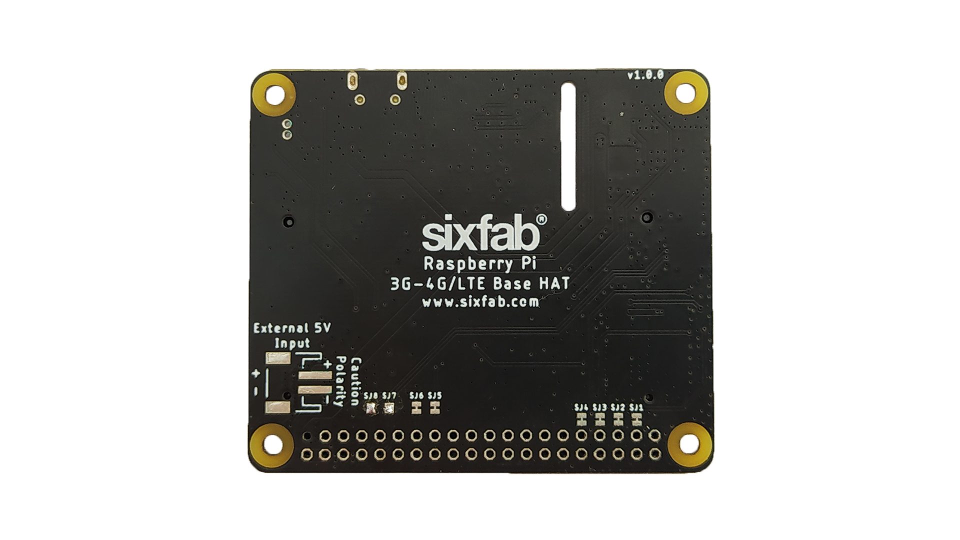
Solder Jumper(SJ)
When you need to communicate with an external electronics over the I2C, you can use these header footprints. The SDA, SCL pins already have 4.7k pull-up resistors.
When you observe the HAT, you will come across some solder Jumpers marked as SJx (SJ1, SJ2, SJX etc)
These solder jumpers are either connected or disconnected by default. These can be used to enable or disable the default use case. These SJ are provided for the cases where the specific GPIO are conflicting with the users requirement. Disconnecting the jumpers may lead to loss in some programmable feature. For instance, Cutting SJ2 which is connected to the power key will take the ability to power on and off from the software. As a result user would need to use the physical button.
Disconnecting:
Cut the narrow trace between the middle of these solder jumper with a utility knife.
Connecting/Reconnecting:
Solder the jumper to connect the traces.
The SJ details for each version of the board are mentioned below.
| Solder Jumper | Corresponding GPIO | Default State | Purpose | Affect of changing the default state |
|---|---|---|---|---|
| SJ1 | GPIO13 | CONNECTED | Cut to disconnect GNSS TX of the module. | Cannot use GNSS over UART4. |
| SJ2 | GPIO12 | CONNECTED | Cut to disconnect GNSS RX of the module. | Cannot use GNSS over UART4. |
| SJ3 | GPIO24 | CONNECTED | Cut to disconnect the POWERKEY from GPIO. | Cannot use Power Button on the program. |
| SJ4 | GPIO23 | CONNECTED | Cut to disconnect the GPIO of STATUS Led. | The Led will work but cannot be read on the program. |
| SJ5 | GPIO22 | CONNECTED | Cut to disconnect USER BUTTON. | Cannot use User Button. |
| SJ6 | GPIO18 | CONNECTED | Cut to disconnect the RESET Button from GPIO. | Cannot use Reset Button on the program. |
| SJ7 | GPIO27 | CONNECTED | Cut to disconnect USER LED. | Cannot use User LED. |
| SJ8 | GPIO17 | CONNECTED | Cut to disconnect ENABLE pin from GPIO. | Cannot control the power of HAT. |
| Solder Jumper | Corresponding GPIO | Default State | Purpose | Affect of changing the default state |
|---|---|---|---|---|
| RX1 | TXD | CONNECTED | Cut to disconnect TX of module. Used to communicate over UART. | Cannot communicate over UART. |
| TX1 | RXD | CONNECTED | Cut to disconnect RX of module. Used to communicate over UART. | Cannot communicate over UART. |
| DIS | GPIO17 | CONNECTED | Cut to disconnect ENABLE pin from GPIO. | Cannot control the power of HAT. |
| U.LED | GPIO27 | CONNECTED | Cut to disconnect USER LED | Cannot use User Led. |
| U.BUT | GPIO22 | CONNECTED | Cut to disconnect USER BUTTON | Cannot use User Button. |
| STAT | GPIO23 | CONNECTED | Cut to disconnect the GPIO of STATUS Led. | The Led will work but cannot be read on program. |
| PKEY | GPIO24 | CONNECTED | Cut to disconnect POWERKEY from GPIO. | Cannot use Power Button on program. |
| TX2 | GPIO12 | CONNECTED | Cut to disconnect GNSS RX of the module. | Cannot use GNSS over UART4. |
| RX2 | GPIO13 | CONNECTED | Cut to disconnect the GNSS TX of the module. | Cannot use GNSS over UART4. |
| SJX/JP1 | NA | NOT CONNECTED | Solder to use Active GNSS antenna connection | Active GNSS antenna can be used. |
Updated 3 months ago